PDF

Modeling of a UHF RFID Tag
Introduction
UHF RFID tags are widely used for identifying and tracking animals. This example simulates a passive radio-frequency identification (RFID) tag for the UHF frequency range.
With respect to the chip transponder’s complex impedance, a reflection coefficient is computed. This is done using an approach that differs from the conventional scattering parameter analysis method by a real reference impedance value.
Figure 1: The RFID tag’s geometry consists of copper traces patterned on an FR4 board that is enclosed by a low dielectric PTFE case. The surrounding air domain and perfectly matched layers, which are required for the simulation, are not included in this figure.
Model Definition
In this example, the RFID tag’s operating frequency is 915 MHz. At this frequency, the metal part of the RFID tag can be modeled as a perfect electrical conductor (PEC), because while the copper traces patterned on the FR4 board are geometrically very thin, they are much thicker than the skin depth.
The entire circuit board is inserted inside a lossless PTFE casing. The tag is modeled in a spherical air domain, which is enclosed by perfectly matched layers (PML) that absorb all outgoing radiation from the tag.
A lumped port with a reference impedance of 50 Ω is used on the location of an RFID chip. This is done to excite the tag and evaluate the input impedance of the tag’s antenna part, which is modeled as a meander line. An additional copper strip is placed adjacent to the meander line to control the impedance.
The conventional S-parameter works well only with a real reference impedance. However, the RFID chip's impedance is complex and the calculated S-parameter is not physical when a complex port reference impedance is used.
In Ref. 1, the power wave reflection coefficient term is introduced. It is applicable for evaluating the matching properties of an RFID tag:
where Zl is the complex load impedance and Zref is the complex reference impedance.
Results and Discussion
Figure 2 shows the default E-field norm on the xy-plane. The field distribution plot indicates that the electric field is symmetrically confined along the meander line, as well as in the area between the meander line and impedance matching strip.
The far-field radiation pattern of the tag is shown in Figure 3. Noticeably, the tag's radiation pattern looks very similar to the radiation pattern of a half-wave dipole antenna.
The evaluated impedance of the tag is around 18 + j124 Ω and the power wave reflection coefficient, in dB, is below 15 dB.
Figure 2: The E-field norm plot shows where the field is strongly confined in the tag.
Figure 3: The far-field radiation pattern resembles that of a half-wave dipole antenna.
Reference
1. K. Kurokawa, “Power Waves and the Scattering Matrix,” IEEE Transactions on Microwave Theory and Techniques, Volume 13, 1965.
Application Library path: RF_Module/Antennas/uhf_rfid_tag
Modeling Instructions
From the File menu, choose New.
New
In the New window, click  Model Wizard.
Model Wizard
1
In the Model Wizard window, click  3D.
2
In the Select Physics tree, select Radio Frequency>Electromagnetic Waves, Frequency Domain (emw).
3
Click Add.
4
Click  Study.
5
In the Select Study tree, select General Studies>Frequency Domain.
6
Study 1
Step 1: Frequency Domain
1
In the Model Builder window, under Study 1 click Step 1: Frequency Domain.
2
In the Settings window for Frequency Domain, locate the Study Settings section.
3
In the Frequencies text field, type 915[MHz].
Global Definitions
Parameters 1
1
In the Model Builder window, under Global Definitions click Parameters 1.
2
In the Settings window for Parameters, locate the Parameters section.
3
Geometry 1
1
In the Model Builder window, under Component 1 (comp1) click Geometry 1.
2
In the Settings window for Geometry, locate the Units section.
3
From the Length unit list, choose mm.
Import 1 (imp1)
1
In the Home toolbar, click  Import.
2
In the Settings window for Import, locate the Import section.
3
Click  Browse.
4
5
Click  Import.
6
Click the  Wireframe Rendering button in the Graphics toolbar.
Add a sphere for the air domain surrounding the RFID tag and perfectly matched layers that will be configured later on.
Sphere 1 (sph1)
1
In the Geometry toolbar, click  Sphere.
2
In the Settings window for Sphere, locate the Size section.
3
In the Radius text field, type 150.
4
Click to expand the Layers section. In the table, enter the following settings:
5
Click  Build All Objects.
6
Click the  Zoom Extents button in the Graphics toolbar.
Definitions
Variables 1
1
In the Model Builder window, under Component 1 (comp1) right-click Definitions and choose Variables.
Define a variable for calculating the reflection coefficient between two complex impedances.
2
In the Settings window for Variables, locate the Variables section.
3
Perfectly Matched Layer 1 (pml1)
1
In the Definitions toolbar, click  Perfectly Matched Layer.
2
These are all of the outermost domains of the sphere.
3
In the Settings window for Perfectly Matched Layer, locate the Geometry section.
4
From the Type list, choose Spherical.
Electromagnetic Waves, Frequency Domain (emw)
Perfect Electric Conductor 2
1
In the Model Builder window, under Component 1 (comp1) right-click Electromagnetic Waves, Frequency Domain (emw) and choose the boundary condition Perfect Electric Conductor.
2
Click the  Zoom In button in the Graphics toolbar, a couple of times to get a clear view of the RFID tag.
3
Lumped Port 1
1
In the Physics toolbar, click  Boundaries and choose Lumped Port.
2
For the first port, wave excitation is on by default.
3
Click the  Zoom Extents button in the Graphics toolbar.
4
Click the  Zoom In button in the Graphics toolbar.
Far-Field Domain 1
In the Physics toolbar, click  Domains and choose Far-Field Domain.
Add Material
1
In the Home toolbar, click  Add Material to open the Add Material window.
2
Go to the Add Material window.
3
4
Click Add to Component in the window toolbar.
5
In the tree, select Built-in>FR4 (Circuit Board).
6
Click Add to Component in the window toolbar.
7
In the Home toolbar, click  Add Material to close the Add Material window.
Materials
FR4 (Circuit Board) (mat2)
Select Domain 7 only.
Material 3 (mat3)
1
In the Model Builder window, right-click Materials and choose Blank Material.
2
3
In the Settings window for Material, locate the Material Contents section.
4
Mesh 1
In the Model Builder window, under Component 1 (comp1) right-click Mesh 1 and choose Build All.
To see the meshed structure of the device, remove some boundaries from the view.
Definitions
Hide for Physics 1
1
In the Model Builder window, right-click View 1 and choose Hide for Physics.
2
In the Settings window for Hide for Physics, locate the Geometric Entity Selection section.
3
From the Geometric entity level list, choose Boundary.
4
Mesh 1
Study 1
Step 1: Frequency Domain
In the Home toolbar, click  Compute.
Results
Multislice
1
In the Model Builder window, expand the Electric Field (emw) node, then click Multislice.
2
In the Settings window for Multislice, locate the Multiplane Data section.
3
Find the X-planes subsection. In the Planes text field, type 0.
4
Find the Y-planes subsection. In the Planes text field, type 0.
5
In the Electric Field (emw) toolbar, click  Plot.
6
Click the  Go to XY View button in the Graphics toolbar.
Zoom in a couple of time to get a good view of the RFID tag.
Compare the reproduced plot with Figure 2.
2D Far Field (emw)
The E-plane radiation pattern resembles that of a dipole antenna.
Radiation Pattern 1
1
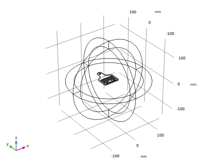
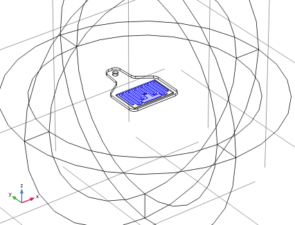
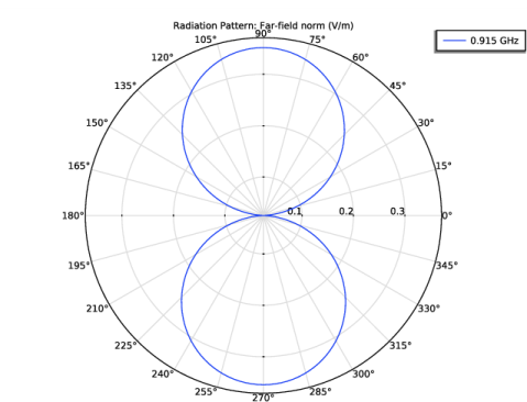
In the Model Builder window, expand the 3D Far Field, Gain (emw) node, then click Radiation Pattern 1.
2
In the Settings window for Radiation Pattern, locate the Evaluation section.
3
Find the Angles subsection. In the Number of azimuth angles text field, type 40.
4
In the 3D Far Field, Gain (emw) toolbar, click  Plot.
Table
1
Go to the Table window.
Reproduce Figure 3.
Results
Global Evaluation 2
1
In the Results toolbar, click  Global Evaluation.
2
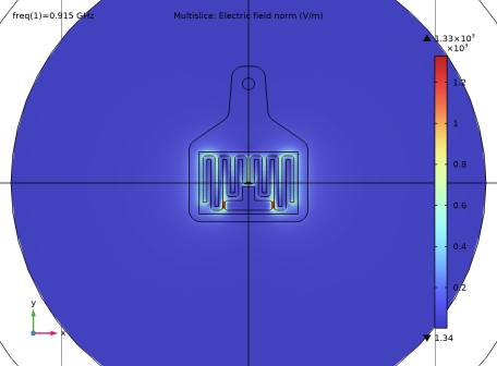
In the Settings window for Global Evaluation, click Replace Expression in the upper-right corner of the Expressions section. From the menu, choose Component 1 (comp1)>Electromagnetic Waves, Frequency Domain>Ports>emw.Zport_1 - Lumped port impedance - Ω.
3
Click  Evaluate.
Global Evaluation 3
1
In the Results toolbar, click  Global Evaluation.
2
In the Settings window for Global Evaluation, locate the Expressions section.
3
4
Click  Evaluate.